Physicists snap first image of an ‘electron ice’
Ninety years after they were first predicted, UC Berkeley researchers show what a solid made of electrons looks like
October 4, 2021
More than 90 years ago, physicist Eugene Wigner predicted that at low densities and cold temperatures, electrons that usually zip through materials would freeze into place, forming an electron ice, or what has been dubbed a Wigner crystal.
While physicists have obtained indirect evidence that Wigner crystals exist, no one has been able to snap a picture of one — until now.
UC Berkeley physicists published last week in the journal Nature an image of just such an electron ice sandwiched between two semiconductor layers. The image is proof positive that these crystals exist.
“If you say you have an electron crystal, show me the crystal,” senior author Feng Wang, Berkeley professor of physics, told Nature.
The Berkeley and Berkeley Lab team, involving physicists from the labs of Wang, Michael Crommie and Alex Zettl, developed a new technique for visualizing the crystals, which tend to “melt” when probed. By placing a graphene sheet over the semiconductor sandwich, the team was able to probe the Wigner crystal with a scanning tunneling microscope without melting the sample and demonstrate the crystalline lattice structure, as Wigner predicted.
According to doctoral candidate Hongyuan Li and former postdoctoral fellow Shaowei Li, co-first authors of the paper, the study not only lays a solid foundation for understanding electron Wigner crystals, but also provides an approach that is generally applicable for imaging correlated electron lattices in other systems.
“The technique is non-invasive to the state you want to probe. To me, it is a very clever idea,” physicist Kin Fai Mak of Cornell University told Nature.
Imaging electron clouds with graphene
Electrons inside materials behave in many strange ways, but almost always zip around at high speed. Wigner predicted that if they could be slowed down, their natural repulsion — particles with the same electric charge repel one another — would allow them to assume a uniformly spaced arrangement, essentially a crystal structure.

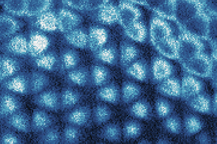
The UC Berkeley researchers used a scanning tunneling microscope tip (top) to image a graphene sheet (pink) that, like photographic paper, recorded the positions of electrons (red) in the Wigner crystal, which formed between two sheets of semiconducting material (blue and green). (UC Berkeley graphic courtesy of Feng Wang’s lab)
The team created the Wigner crystals making a sandwich of single-atom layers of two similar semiconductors: tungsten disulfide and tungsten diselenide. The researchers used an electric field to tune the density of the electrons between the two layers and then cooled the entire device to a temperature of about 5 Kelvin, near absolute zero.
Their first attempt to measure the electron density in the two-dimensional crystal sandwich with a scanning tunneling microscope (STM) destroyed the crystal. The team suggested covering the device with a graphene sheet, which acts like a sheet of photo paper to record the location of the electrons. The scientists used the STM to read the electron image on the graphene — as predicted, the electrons settled into a crystal arrangement with a separation nearly 100 times greater than the separation of atoms in the semiconductor sheets.
Other co-authors of the paper are Emma Regan, Danqing Wang, Wenyu Zhao and Salman Kahn of Berkeley; Kentaro Yumigeta, Mark Blei and Sefaattin Tongay of Arizona State University in Tempe; and Takashi Taniguchi and Kenji Watanabe of the National Institute for Materials Science in Tsukuba, Japan. The work was funded primarily by the U.S. Department of Energy (DE-AC02-05-CH11231).